3D Interferometric-Sensors
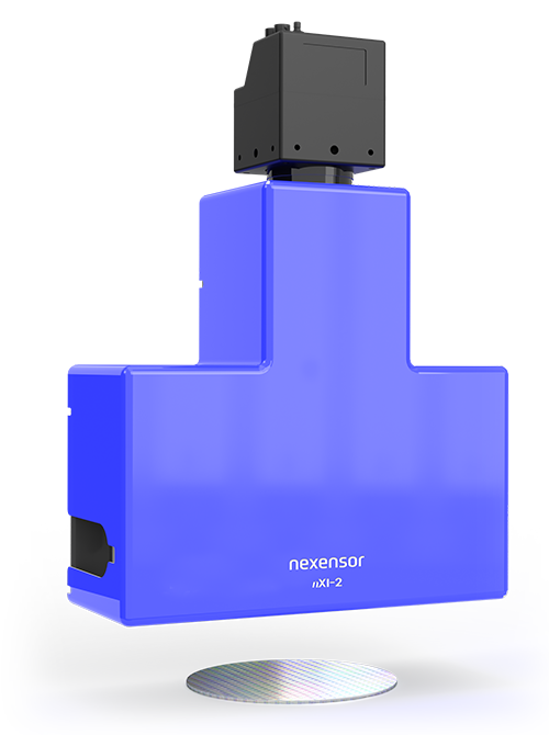
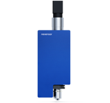
nXI-2
Interferometer sensor
for large areas
for large areas
Thin-film separation and ultra-high-speed
and ultra-precise shape measurement of large-area products
and ultra-precise shape measurement of large-area products
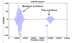
nXI-2 adopts interferometry, a technology used to calibrate precision measuring
equipment and deliver precision measurement of large areas. While generating
a mass amount of data, nXI-2 measures ten times faster than
the conventional interferometry method and provides reliable data,
thus delivering various information to improve process efficiency
and production quality. Because it can measure a wide area at a fast speed,
nXI-2 is the right fit for mass production lines and, its advanced
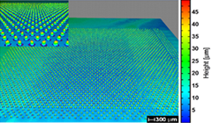
measuring technology ensures high reliability of measurements. nXI-2 measures step, thickness, and roughness, and hence can use for measuring spots
of an ㎛ or less, such as the microstructures, bumps, and roughness of semiconductors,
and the column spacers, surface structures, and protrusions by foreign substances
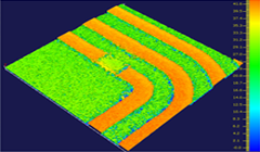
in displays, etc. In addition, it can separate thin films and so excels in measuring products
with multilayer structures. nXI-2 measures up to FOV 33 ㎜ × 22 ㎜
and hence is used to measure various products.
equipment and deliver precision measurement of large areas. While generating
a mass amount of data, nXI-2 measures ten times faster than
the conventional interferometry method and provides reliable data,
thus delivering various information to improve process efficiency
and production quality. Because it can measure a wide area at a fast speed,
nXI-2 is the right fit for mass production lines and, its advanced
measuring technology ensures high reliability of measurements. nXI-2 measures step, thickness, and roughness, and hence can use for measuring spots
of an ㎛ or less, such as the microstructures, bumps, and roughness of semiconductors,
and the column spacers, surface structures, and protrusions by foreign substances
in displays, etc. In addition, it can separate thin films and so excels in measuring products
with multilayer structures. nXI-2 measures up to FOV 33 ㎜ × 22 ㎜
and hence is used to measure various products.
Key Features
· Large area measuring
FOV 33 ㎜ × 22 ㎜
· A high- resolution
image sensor
(4000 X 3000 pixel resolution)
FOV 33 ㎜ × 22 ㎜
· A high- resolution
image sensor
(4000 X 3000 pixel resolution)
· Applicable to the mass production line
· Fast processing of high- resolution images
· Fast processing of high- resolution images
· Simple SW interface
· Real-time measurement sharing by shared memory
· Real-time measurement sharing by shared memory
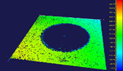
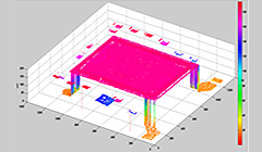
Application
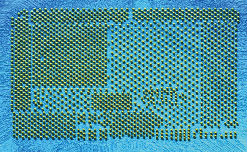
Wafer Bumps
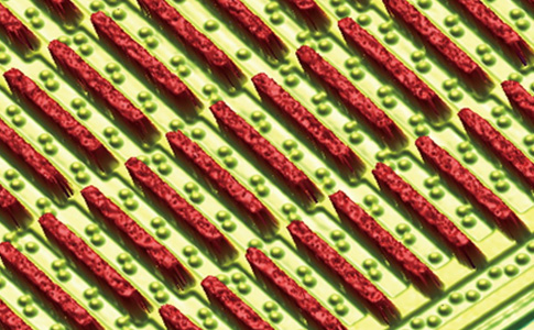
DDI
HBM
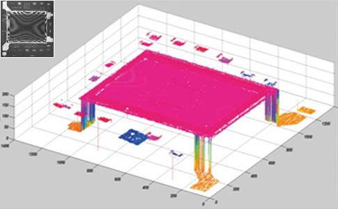
Image Sensor
Specifications
Request a specification
Contact us
Latest News


Request a sample test
Request a sample test now!
You can experience the technology of Nexensor.
You can experience the technology of Nexensor.
Contact us
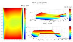
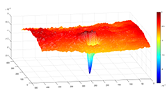
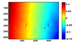
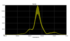
| Measuring model | Measuring technology | Test content | Measuring data |
|
Large-area measurement with WSI interferometers FOV extensive application | Micro Bump Height Monolayer membrane thickness measurement PCB fine pattern Processed surface roughness measurement Sensor step-difference measurement |
|
|
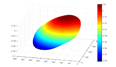
Free-Form Metrology
Divided inspection possible according to product curve angels
|
Inspection of lens and glass, and measurement of shapes
Inspection of OLED surfaces, and measurement of shapes
Inspection of wafer surfaces, and measurement of shapes
|
|
|
Real-time measurement of transparent and semitransparent product thickness
Applicable to multi-channels
|
Measurement of wafer(silicone, sapphire) thickness
Measurement of glass and film thickness
|
|