Critical Dimension Measuring
nXD-1
High-resolution optical system
150㎚ resolution, real-time 2D/3D measurement solution
of micro-patterns to overcome the diffraction limit
of micro-patterns to overcome the diffraction limit
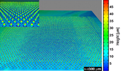
nXD-1 overcomes the inherent measurement limitations of conventional optical
structures. Due to the diffraction limit, CD line widths of 1 ㎛ or less were measured
only by a scanning electron microscope, which requires special equipment. However, nXD-1 uses an optical system and algorithm to get over the diffraction limit
and accurately measure a line width of 1 ㎛ with an optical resolution of 100 ㎚.
If you need to measure CD line width of 1 ㎛ due to the miniaturization and
high integration of semiconductor chips, measuring with the non-destructive
optical structure will open up a new horizon. In addition, if you need to measure a fine line width made by using a Femto laser
in the display process, nXD-1 can be the best tool to increase the stability of
the process and deliver precise measurement. Thus, it will usher in a new paradigm
in the measurement market to solve the issues of precise measurement
at the borderline between optical systems and electron microscopes.
Key Features
· Measurement
of fine line width (1㎛)
of fine line width (1㎛)
· Fast measuring and data acquisition
· High precision
· High precision
· Simple measurement process
· Easy user interface
· Minimum installation space
· Easy user interface
· Minimum installation space
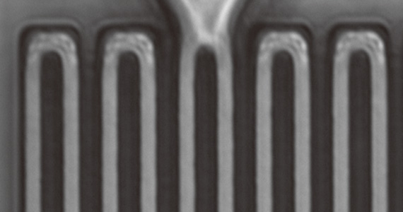
Critical Dimension Measurment
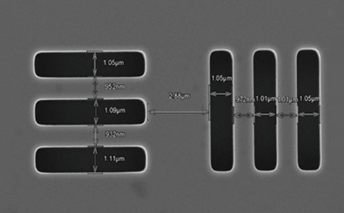
SEM
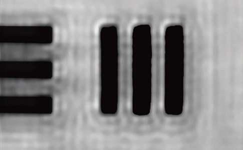
nXD-1 (50x)
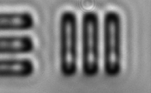
General microscope (50x)
nXD-1 (50x)

General microscope (50x)
Specifications
Request a specification
Contact us
Latest News


Request a sample test
Request a sample test now!
You can experience the technology of Nexensor.
You can experience the technology of Nexensor.
Contact us
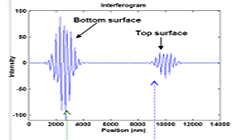
| Measuring model | Measuring technology | Test content | Measuring data |
|
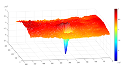
Large-area measurement with WSI interferometers FOV extensive application | Micro Bump Height Monolayer membrane thickness measurement PCB fine pattern Processed surface roughness measurement Sensor step-difference measurement |
|

|
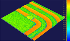
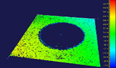
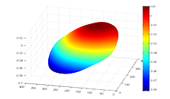
Free-Form Metrology
Divided inspection possible according to product curve angels
|
Inspection of lens and glass, and measurement of shapes
Inspection of OLED surfaces, and measurement of shapes
Inspection of wafer surfaces, and measurement of shapes
|
|
|
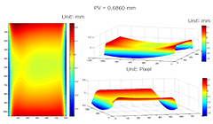
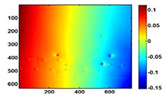
Real-time measurement of transparent and semitransparent product thickness
Applicable to multi-channels
|
Measurement of wafer(silicone, sapphire) thickness
Measurement of glass and film thickness
|
|